 |
| 4256ZE Breakout Board with CLK PCB Operating |
"The ispMACH 4256ZE Breakout Board is a simple, low-cost board that provides convenient access to densely-spaced IOs. Each I/O on the device is connected to 100-mil header holes. By adding test probes, jumper wires, or pin headers to the board, you can easily evaluate function and performace of the IO cells of the ispMACH 4256ZE."
The only issue I have with this board is that unlike its more modern version, the MachXO2 Breakout Board (note that its IOs are only 3.3V tolerant), it has no site for an external clock crystal on the PCB. This means you are limited to the internal 5MHz oscillator. Or not if you are clever and have access to PCB design software and are willing to spend $1 with OSH Park community PCB service.
The Oscillator series chosen for this project was the Fox FXO-HC53 series, a SMT crystal measuring 5mm by 3.2mm. Since this chip doesn't support LVDS we are using a HCMOS output. The two speeds chosen were 80MHz and 200MHz.
Note the oscillator is specified to drive up to 15pF and a CLK input pin on the ispMACH 4256ZE is 6pF max. The traces on the board are going to contribute further capacitance but it should be within spec.
The board design is detailed below:
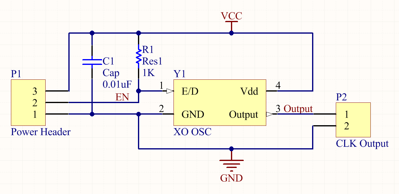 | ||
| CLK Board Schematic |
- The output pin of the oscillator is placed as close as possible to the output pin hole and the ground pin hole is as close as possible to the ground pin of the oscillator. This is to minimize impedance and coupling of the high frequency on the board.
- There are two ground pins - one for the power supply and the other for the CLK return current to make it easier to interface.
- A pullup resistor 0805 position is available in case the internal pullup proves insufficient or a different crystal is chosen.
- The footprint of the crystal has the pad size extended outside the normal footprint by twice the length to allow manual soldering.
- The power and output pins are in a row on a 0.1" spacing to allow compatibility with standard prototyping boards and systems.
- The bottom of the board under the crystal and high frequency traces is one large ground plane.
- Total board size is 525mil x 375mil.
 |
| CLK Board Top Layer |
 | |
| CLK Board Bottom Layer (Text not reversed) |

 |
| OSH Park Rendering of the Manufactured PCB |

